
Back to Electron Microscopy Facility

JEOL NEOARM Low kV STEM Corrected
Contact: Dr. Xun Zhan
Email: xun.zhan@austin.utexas.edu
Location: EER 0.762
Equipment Type:
Electron Microscopy
Transmission Electron Microscopy (TEM)
Instrument Capabilities
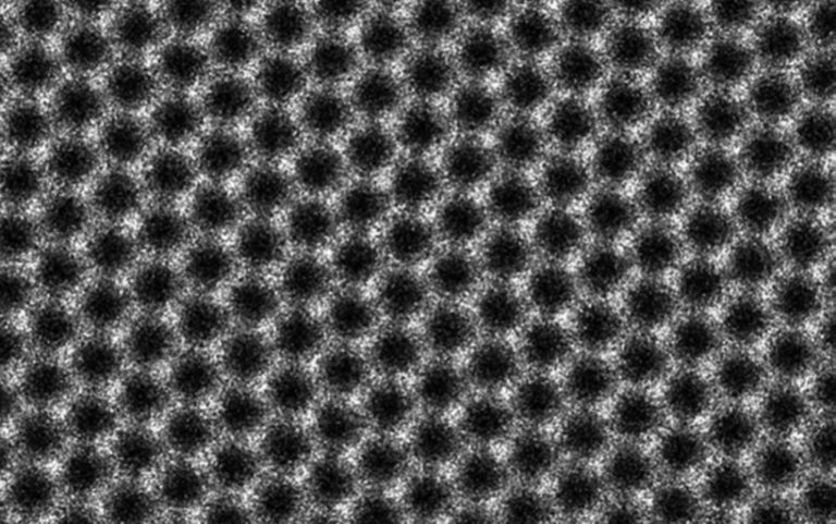
The JEOL NEOARM is a probe-corrected transmission electron microscope with aberration correction from 30 kV to 200 kV.
Key Features
- Atomic-level imaging at 30 kV, 80 kV and 200 kV in STEM
- Atomic-level elemental mapping (EDXS and EELS)
- Electric binding state and plasmon mapping (EELS)
- Energy filtered imaging
- In situ liquid cell, heating and biasing
- Auto tune for fast alignment
Specifications
- Imaging Modes: TEM/STEM
- Voltage: 30 kV to 200 kV
- STEM resolution: 0.0783 nm (200 kV)/ 0.1108 nm (80 kV)/ 0.1920 nm (30 kV)
- Energy resolution: sub 0.3 eV
- Point to Point Resolution TEM: 0.023 nm (200 kV)
- Source: Cold Field Emission
- Tilt Range: 80° (with high tilt holder)
- Lorentz lens
Attachments/Accessories
- Hybrid high angle annular dark field detector
- Annular bright field detector
- Gatan OneView Camera with IS video software (up to 300 fps)
- JEOL large angle silicon drift EDS detector (0.96 sr)
- Gatan Quantum energy filter with DualEELS
- Protochips Fusion Heating/Biasing Holder and Poseidon Liquid Cell
- High tilt holder
- Double-Tilt Holder
Fees and Policies
- UT Users: $130/hour
- Higher Education/State Agencies: $283/hour
- Corporate/External Users: $283/hour
Traning
Users should register for the required in-person training course through UTLearn.
TMI: TEM mode imaging on the JEOL NEOARM aberration-corrected TEM
TMI: XEDS/EELS Analysis on the JEOL NEOARM aberration corrected TEM
TMI: STEM mode imaging on the JEOL NEOARM aberration-corrected TEM
